

Table of contents
Introduction:-
AT89S52 is a microcontroller IC based on 8051 architecture. It contains all the features of the 8051 microcontroller and also some additional features. AT89S52 is a low-power, high-performance, CMOS 8-bit microcontroller with 8K bytes of in-system programmable flash memory. Here what in-system programmable( ISP ) means is that we do not need any external device to erase and rewrite the flash memory. It already has an in-build program for it. This feature makes the development fast and easy. It has many more features we will talk about them and its' programming in the upcoming blogs. Till then stay tuned.
- I highly recommend reading Atmel's datasheet on AT89S52
Features:-
8K bytes of ISP flash memory
- Endurance 1000 write/Erase cycles
256 bytes of internal RAM
32 I/O ports
Three 16-bit Timer/counter.
8 interrupt sources
Full duplex UART serial channel
Watchdog Timer
Dual data pointer
Power off flag
4V to 5.5 V operating range
- The on-chip flash allows us to program the memory in-system or by conventional nonvolatile memory programmer.
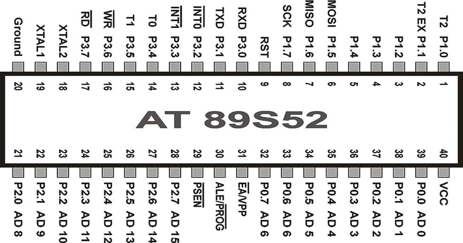
Pin Description:-
VCC
- Supply voltage
GND
- Ground
Port0
8-bit bidirectional open drain I/O port.
As an output port each pin can sink upto 8 TTL inputs. When ones are written to port 0 pins, the pins can be used as a high impedance inputs.
PO can be configured as a data bus during access to an external program or data memory.
P0 also receives the code bytes during flash programming and outputs the code bytes during program verification.
Port1
Port 1 is a bidirectional I/O port with internal pull-ups.
The port 1 output buffers can sink/source 4 TTL inputs.
If as an input port 1 pins are externally pulled low then P1 will source current because of the internal pullups.
Port1 has additional functionalities to some of its' pins. It can be referred from the table.
| Port Pin | Alternate Functions | | --- | --- | | P1.0 | T2 (external count i/p to timer/counter2, clockout | | P1.1 | T2EX (Timer/Counter2 capture reload trigger and direction control | | P1.5 | MOSI (used for ISP (in-system programming) | | P1.6 | MISO (used for ISP) | | P1.7 | SCK ( used for ISP) |
Port2
Port2 is an 8-bit bidirectional I/O port with internal pullups.
Port2 output buffers can sink/source 4 TTL inputs.
As an input P2 pins that are externally pulled low, will source current because of the internal pull-up resistor.
P2 also receives the high-order input bits and some control signals during flash programming and verification.
Port3
Port3 is a 8-bit bidirectional I/O port with internal pullups.
P3 output buffers can sink upto 4 TTL inputs.
P3 receives some control signals for flash programming and verification.
P3 also serves the functions of various special features as shown in the table.
| Port Pin | Alternate Functions | | --- | --- | | P3.0 | RXD (serial input port) | | P3.1 | TXD (serial output port) | | P3.2 | INT0 (external interrupt 0) | | P3.3 | INT1 (external interrupt 1) | | P3.4 | T0 (timer 0 external input) | | P3.5 | T1 (timer 1 external input) | | P3.6 | WR ( external data memory write strobe) | | P3.7 | RD ( external data memory read strobe) |
RST
- Reset input. A high on this pin for two machine cycles while the oscillator is running resets the device.
ALE/PROG
Address latch enable is an output pulse for latching the low byte of the address during accesses to external memory.
This pin is also the program pulse input during flash programming.
In normal case, ALE is continuously emitted at 1/6 frequency of the oscillator.
PSEN
Program store enable is read strobe to the external program
When AT89S52 is executing code from external memory PSEN is activated twice each machine cycle.
EA/ VPP
External Access Enable. EA must be strapped to GND to enable device to fetch code from external memory locations starting at 0000H up to FFFFH.
EA should be connected to VCC for internal program execution
This pin also receives 12 V programming enable voltage(Vpp) during flash programming.
XTAL1
- Input to the inverting oscillator amplifier and input to the internal clock operating circuit.
XTAL2
- Output from the inverting oscillator amplifier
In the upcoming blog, I will be writing about SFRs ( special function registers), memory management, and many such topics related to this microcontroller IC.
If there are any suggestions or any mistakes in the blog, other than grammatical errors please feel free to write in the comments.